Abstract
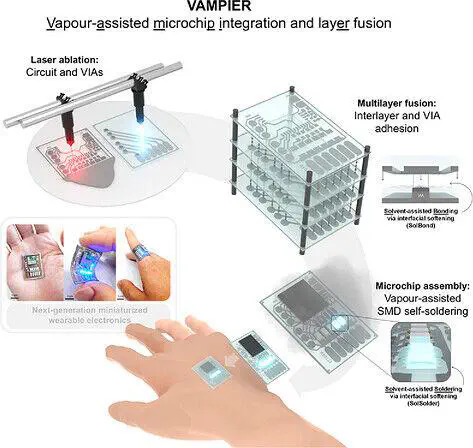
ABSTRACT Soft‐matter electronics offer compelling opportunities for digital health, soft robotics, and interactive systems; however, their translation beyond laboratory remains limited by the absence of fabrication approaches that achieve PCB‐like circuit resolution, reliable microchip integration, and multilayer interconnects, while preserving mechanical compliance, stretchability, and ultralow thickness. We present a scalable fabrication platform for high‐resolution, multilayer soft‐PCBs that combines solvent‐mediated interfacial engineering on reversible polymers, material‐selective laser‐assisted patterning with feature sizes down to ∼25 µm, laser‐assisted VIA formation, and biphasic liquid‐metal‐based conductive composites. We introduce Vapor‐Assisted MicrochiP Integration and layER fusion (VAMPIER), a unified process enabling both microchip attachment and multilayer lamination. VAMPIER exploits solvent‐induced interfacial softening for layer bonding (SolBond) and microchip soldering (SolSolder). VAMPIRE induces a transient transform of physically cross‐linked elastomers into a gel state, promoting conformal contact, interlayer fusion, and robust electrical coupling. This results in low‐resistance microchip pad‐to‐interconnect junctions and reliable VIA connections without thermal soldering. A planarization strategy ensures layer flatness prior to fusion, improving yield and interconnect reliability. All fabrication steps are performed below 60°C, enabling compatibility with soft polymers and surface‐mount devices. This platform enables multilayer, microchip‐integrated soft‐PCBs approaching rigid PCB standards in resolution and density, while offering superior mechanical resilience and sustainability.