Digitally printed stretchable electronics: a review.
Daniel Fernandes
Carmel Majidi
Mahmoud Tavakoli
Stretchable electronics are becoming an important branch in the field of electronics, with a rapidly growing number of studies on highly deformable circuits that can handle large tensile strains without losing electronic functionality.
Digital printing methods such as Inkjet printing, 3D printing and laser ablation are especially attractive since they can be automated and eliminate the need for a stencil, mask or clean-room lithography.
This article reviews recent advances in digital fabrication of stretchable circuits using either additive techniques, that allow
direct printing of certain materials with a determined shape, or subtractive methods, in which the desired pattern is obtained by selectively removing parts of a greater film. For most of the materials used in stretchable electronics, these fabrication methods can be simple to implement, low cost, scalable over large areas, compatible with a broad variety of materials and have a size resolution that is comparable to conventional PCB manufacturing.

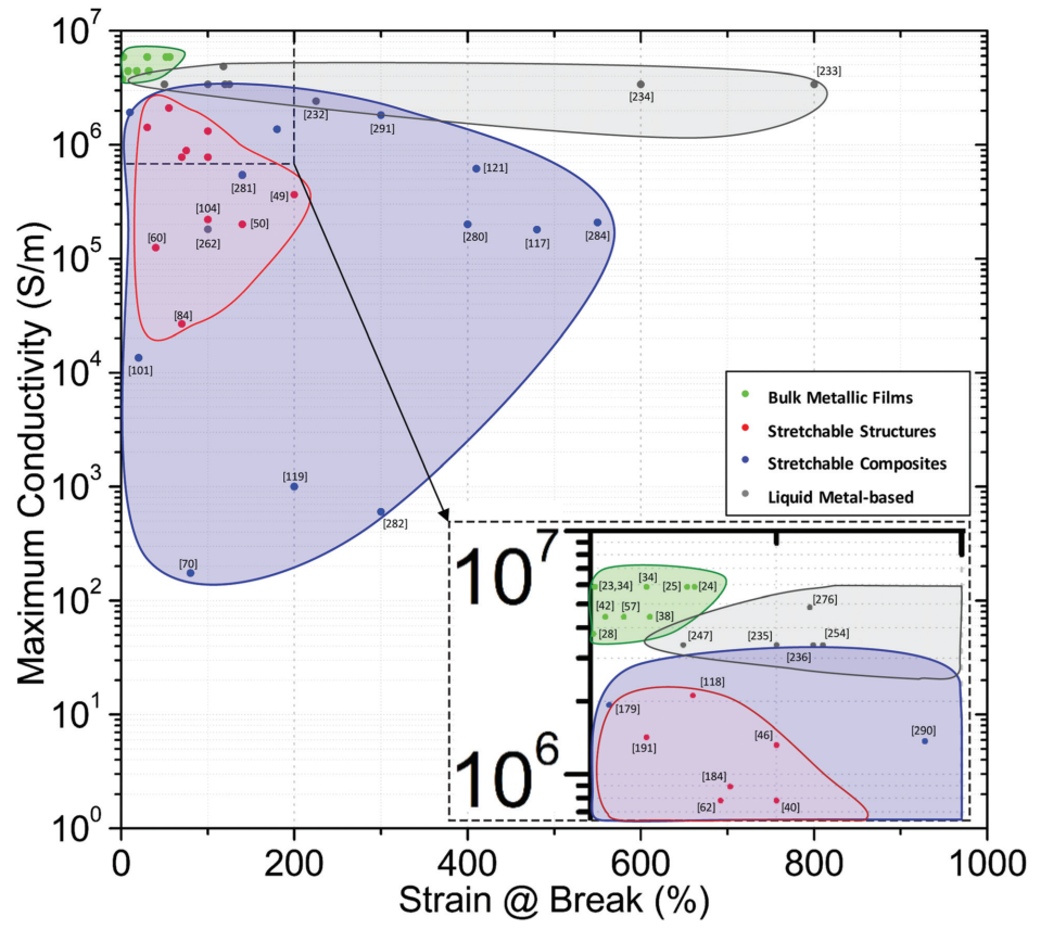
Ashby graphic displaying the published works of stretchable concepts/applications in terms of their maximum conductivity and strain at their breaking point.
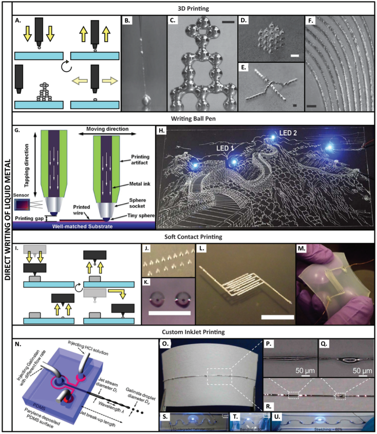
Liquid metal-based stretchable applications by means of Direct Writing. (A–F) Extruded EGaIn beads to assemble 3D structures.259 (G and H) EGaIn-filled ballpoint pen to enable to production of 2D custom patterns.262 (I–M) Soft contact printing of EGaIn patterns with a soft PDMS needle, enabling (L and M) the production of a capacitive sensor.250 (N) InkJet printing of Galinstan with a custom-made print head. It is composed of coplanar channels, filled separately with liquid metal and an HCl solution, in a parylene-coated PDMS piece. This apparatus enabled the deposition of (O–R) straight tracks with minimum widths of approximately 50 mm and (S) serpentine tracks that could be considerably (T) bent and (U) stretched without any significant loss of conductivity.265 Scale bars: 500 mm (C–F), 1 mm (K), 5 mm (L). All images reproduced with permission.

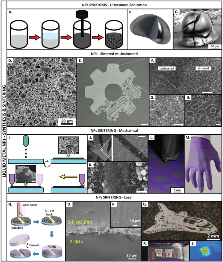
Liquid metal NPs synthesis, sintering and applications. (A) LM NPs are generated by ultrasound in which bulk LM is submerged in a certain solvent and sonicated to obtain the (B) particles. By default, these LM fragments are encapsulated by (C) an innate semiconductive oxide layer.241 (D) This shell prevents subsequent agglomeration but also the electron flow276 and (E–H) sintering is necessary to enable it, promoting the (H) coalescence of the conductive liquid content of the NPs, thus attaining its bulk metal-like conductivity.275 (I) Mechanical sintering is one of the solutions for this problem by mechanically breaking the oxide shells through pressure-induced forces using, for example, (J and K) a diamond probe. (L and M) The authors also reported the InkJet printing of custom patterns with LM NPs-based ink in a common nitrile glove.275 (N–S) Another sintering methodology is done using a laser source with a wavelength able to break the oxide layer. (N–P) In this work, PDMS was poured on the exposed LM patterns, i.e., exposed by laser, and lifted off in the end. (Q) Personalized patterns could be sintered and (R and S) a stretchable heater was conceived.276 Scale bars: 2 mm (E); 10 mm (F); 1 mm (G and H); 20 mm (J); 500 nm (K). All images reproduced with permission.
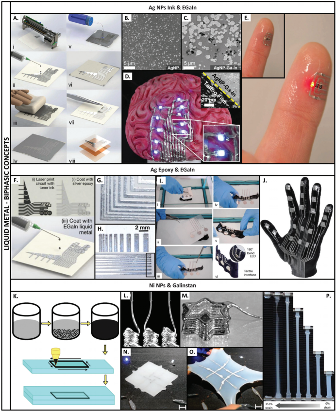
Biphasic systems composed of liquid metal and a solid material implemented in stretchable applications. (A–E) EGaIn alloy of Ag NPs-based patterns delivered by InkJet. (A) The process begins with (i) the pattern print by InkJet, (ii–iv) followed by the EGaIn alloy, i.e., rubbing against the pattern. (iii) This final step binds the liquid metal with the Ag patterns, thus promotes a selective coating. Afterwards, (v and vi) the excessive EGaIn is removed with a wash of acetic solution, followed by (vii) the placement of components, (viii) finishing the process. (B and C) The biphasic layer can be printed on Tattoo Paper and (D and E) delivered on non-flat surfaces through an hydrographic transfer step.277 (F–J) Another approach of biphasic systems with liquid metal was proposed by the same authors (F) using (i) a laser printer, (ii) a coating of an Ag epoxy and (iii) EGaIn rubbing. The EGaIn had the same objective, i.e., (G and H) to promote the selective coating, and the ability to deliver these custom patterns on non-flat surfaces is equivalent to the previous, i.e., through hydrographic transfer.6 (K and L) A extrusion-based system was used to print a composite of solid Ni NPs and Galinstan, delivering personalized (M) 3D structures and (N–P) encapsulated stretchable arrays of this mixture.278 Scale bars: 2 cm (N and O). All images reproduced with permission.

Digitally printed stretchable electronics: a review.
D. Fernandes, C. Majidi, M. Tavakoli, “Digitally printed stretchable electronics: a review.” in Journal of Materials Chemistry C. doi: 10.1039/C9TC04246F.


