

High Resolution Soft and Stretchable Circuits with PVA/Liquid-Metal Mediated Printing.
André F. Silva
Hugo Paisana
Tânia Fernandes
Joana Góis
Arménio Serra
Jorge F. J. Coelho
Aníbal T. de Almeida
Carmel Majidi
Mahmoud Tavakoli
A novel technique that permits, for the first time, fabrication of stretchable traces with linewidths as low as 20 µm and line-spacing of 30 µm, based on simple coating and printing techniques, performed entirely at ambient condition, is demonstrated. By relying on the existing inkjet printing technique, the proposed sinter-free method is a step toward scalable fabrication of high-resolution stretchable circuits, with application in logic gates, transparent conductors, and solar panels.
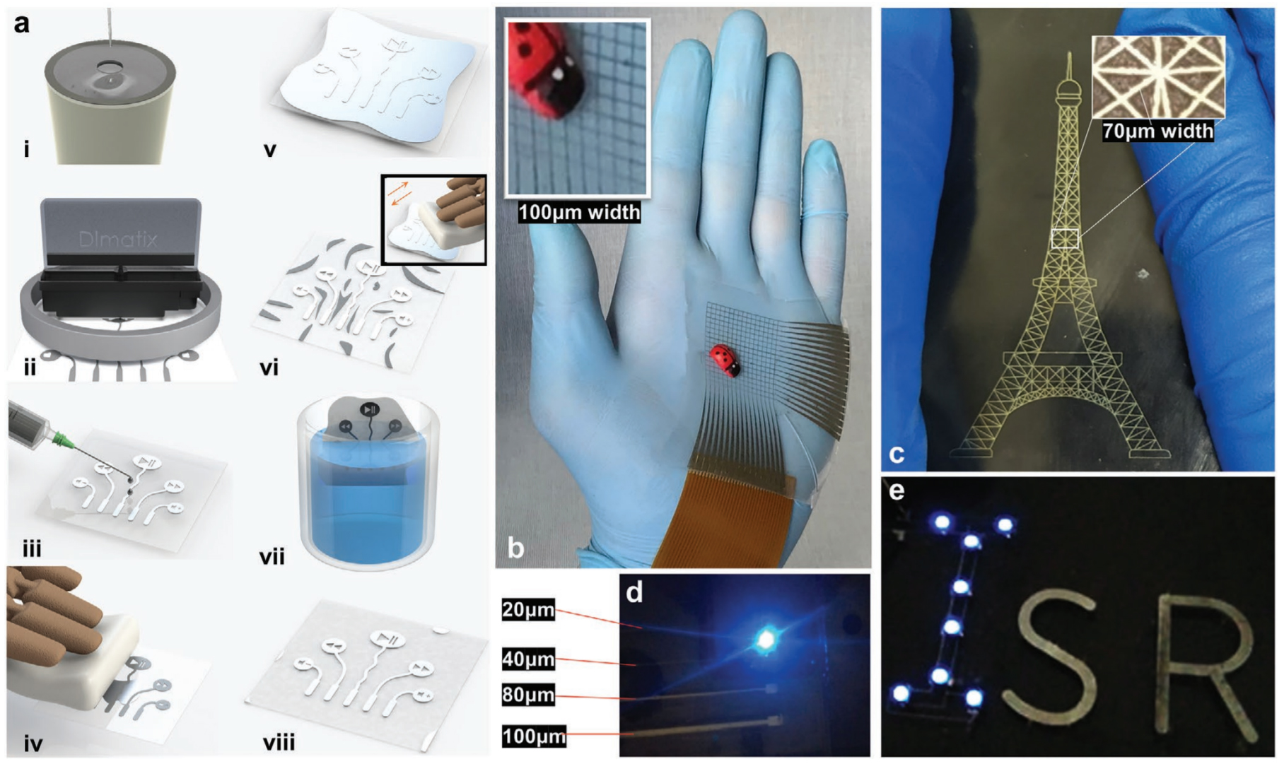
Stretchable Circuit Inkjet printing method and applications. a) Printing procedure for the conductive tracks. Starting from the spin coating method of PVA (i), inkjet printing (ii), alloy, and cleaning process (iii–ix). The step-by-step fabrication process is described in Table S1 and Video S1, Supporting Information). b–e) Various examples of applications with different line width.
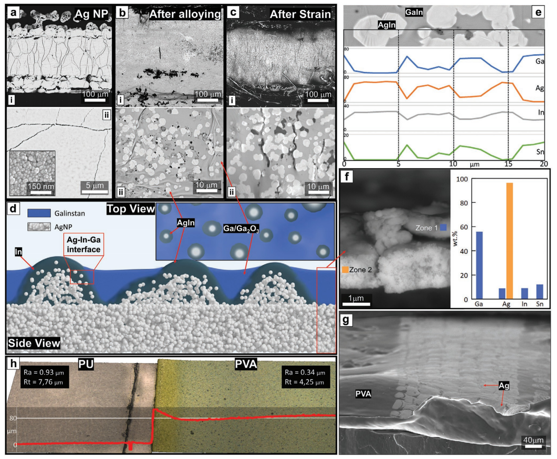
SEM images and schematics. a) Image of a printed trace of AgNPs at various magnifications (SEM backscattered electron (BSE)) (a.i 100 µm scale bar; a.ii 5 µm scale bar). (a.ii.inset) AgNPs image captured using secondary electrons (SEM SE) (150 µm scale bar). b) Trace of silver after treatment at various magnifications (SEM BSE) (b.i 100 µm scale bar; b.ii 10 µm scale bar). c) The effect of straining on the structure with 100 cycles at 30% strain (SEM BSE) (c.i 100 µm scale bar; c.ii 10 µm scale bar). d) Schematics of the Ag-In-Ga relation. e) EDS analysis in line for one treated sample (SEM BSE). f) Cross-section of a treated sample with EDS analysis (SEM BSE). (1 µm scale bar). g) Example of an Ag track with a defect on the PVA (SEM SE) (40 µm scale bar). h) IFM analysis for a sample of PU (left) with five layers of PVA (right). Prepared by separating the PU with tape when coating it with PVA. The graphic (red) contains the profile height of the sample and the text boxes the roughness of the surfaces.
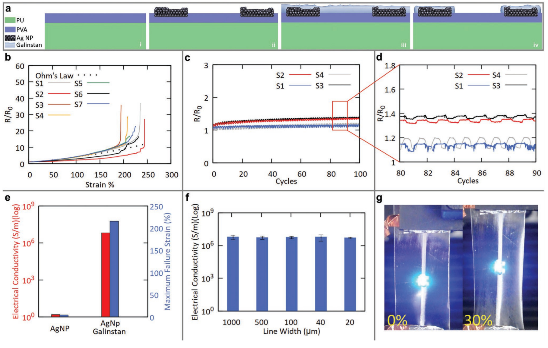
Electromechanical characterization. a) Schematics of layer deposition during the whole process. b) Graphic for the results of the electromechanical test of the maximum rupture strain of seven samples (sample information in Figure S14, Supporting Information). Theoretical behavior represented by the Ohm’s law in dashed. c) Graphic containing the results of the electromechanical test for 30% strain during 100 cycles and d) detail for the zone of 80–90 cycles (sample information in Figure S15, Supporting Information). e) Representation of maximum failure strain (%) and electrical conductivity before and after treatment. f) Graphic with the results of the electrical conductivity for various line widths. g) Image representing the difference in one sample with 0% and 30% strain, respectively (Video S4, Supporting Information).
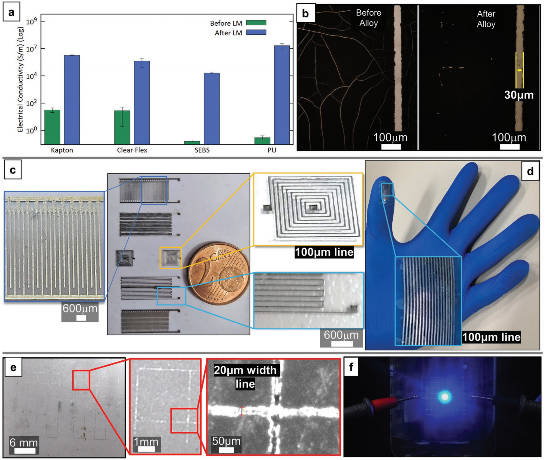
Printing with different substrates and applications. a) Graphic representing the electrical conductivity for treated lines on various substrates. b) Example of lines printed with 30 µm spacing between them before and after coating with Galinstan (100 µm scale bar). c) Example of applications, printed capacitor, strain gauge, and a coil (600 µm scale bars). d) Example of a strain gauge applied on a hand. e) 20 µm line mesh printed at different magnifications. With the naked eye, the lines seem near imperceptible (scale bars left to right: 6 and 1 mm, and 50 µm). f) Example of a mesh with an LED turned on, applied to a curved surface.
High Resolution Soft and Stretchable Circuits with PVA/Liquid‐Metal Mediated Printing.
Francisca M. Carvalho, Pedro Lopes, Manuel Carneiro, Arménio Serra, Jorge Coelho, Aníbal T. de Almeida, Mahmoud Tavakoli, Nondrying, Sticky Hydrogels for the Next Generation of High-Resolution Conformable Bioelectronics, ACS Applied Electronic Materials, 10.1021/acsaelm.0c00653, (2020).