Bi-Phasic Ag-In-Ga-Embedded Elastomer Inks for Digitally Printed, Ultra-Stretchable, Multi-layer Electronics
Pedro Alhais Lopes
Daniel Félix Fernandes
André F. Silva
Daniel Green Marques
Aníbal T. de Almeida
Carmel Majidi
Mahmoud Tavakoli
A bi-phasic ternary Ag−In−Ga ink that demonstrates high electrical conductivity, extreme stretchability, and low electromechanical gauge factor (GF) is introduced. Unlike popular liquid metal alloys such as eutectic gallium−indium (EGaIn), this ink is easily printable and nonsmearing and bonds strongly to a variety of substrates. Using this ink and a simple extrusion printer, the ability to perform direct writing of ultrathin, multi-layer circuits that are highly stretchable , have excellent conductivity, and exhibit only a modest GF (0.9) related to the ratio of percent increase in trace resistance with mechanical strain is demonstrated. The ink is synthesized by mixing optimized quantities of EGaIn, Ag microflakes, and styreneisoprene block copolymers, which functions as a hyperelastic
binder.

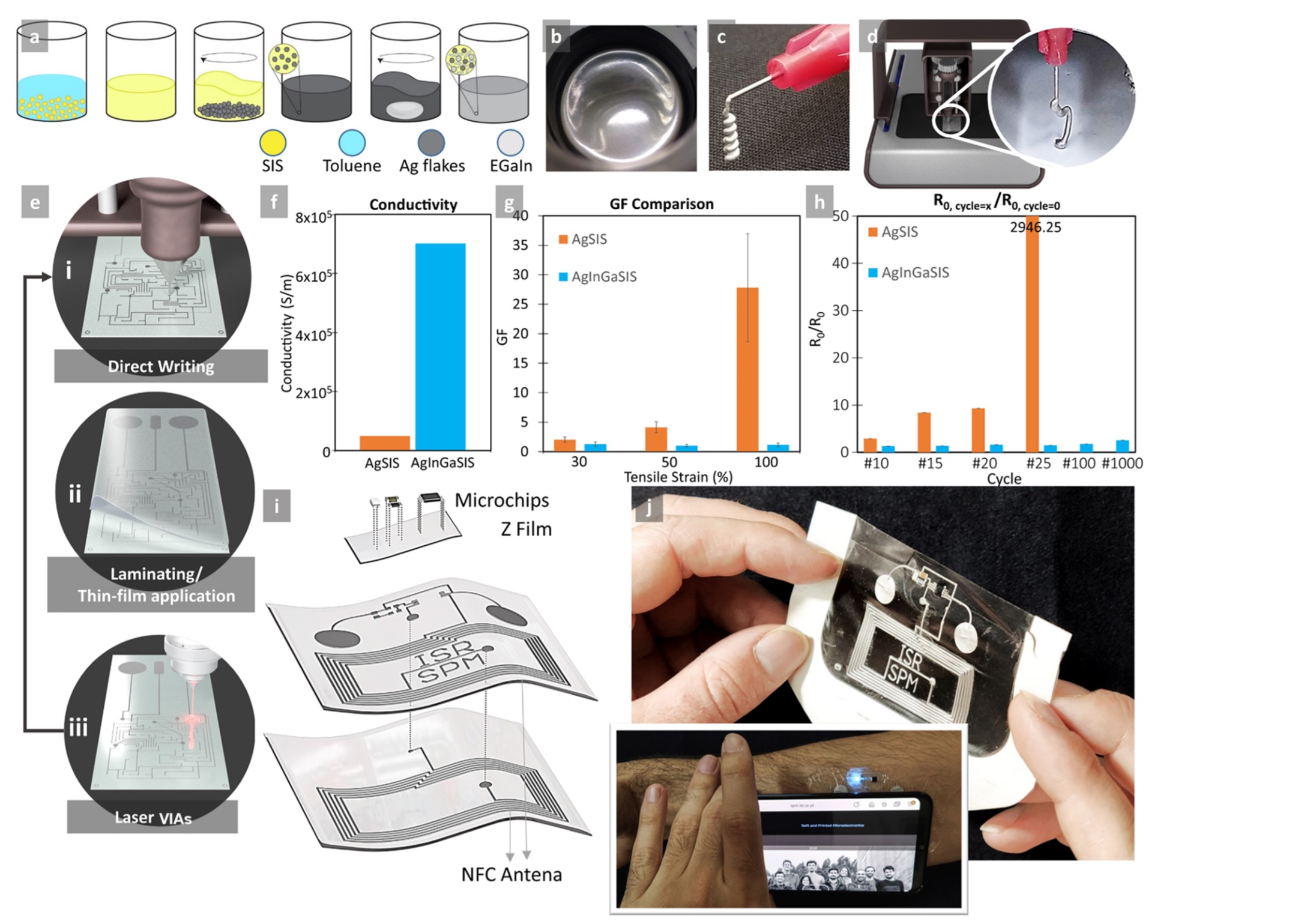
AgInGa-SIS ink synthesis and printing. (a) The ink is synthesized by first dissolving SIS in toluene, followed by the addition and mixing of Ag flakes and EGaIn. (b) The final result ink has coherent and shiny appearance. (c) The ink rapidly forms a solid structure after coming out of the nozzle. (d) A simple extrusion-based printer is used for the printing of stretchable inks. The inset shows the possibility of extrusion of small free-standing geometries. (e) Three fabrication steps for printing multi-layer circuits includes, (i) direct writing (digital printing), (ii) laminating a layer of a prefabricated polymer or application of a thin film of a prepolymer using a thin-film applicator. (iii) Electrical VIAs are created using a CO2 laser or by drilling. These steps can be repeated for making multi-layer circuits. (f) Conductivity of the AgInGa ink compared to the AgSIS ink. (g) GF comparison between the two inks at 30, 50, and 100% strain. (h) R0, cycle = x/R0, cycle = 0 (0% strain) at different cycles during cycle tests. (i) Representation of a battery-free multi-layer NFC circuit, with a double-layer antenna for high-efficiency energy harvesting. Microchips are interfaced to the circuit using an anisotropic conductive film. (j) Printed NFC circuit over a medical-grade Tegaderm adhesive, transferred to the forearm. Inset image: when a mobile phone approaches the circuit, it lights an LED on the circuit and opens the SPM-ISR website in the mobile phone.

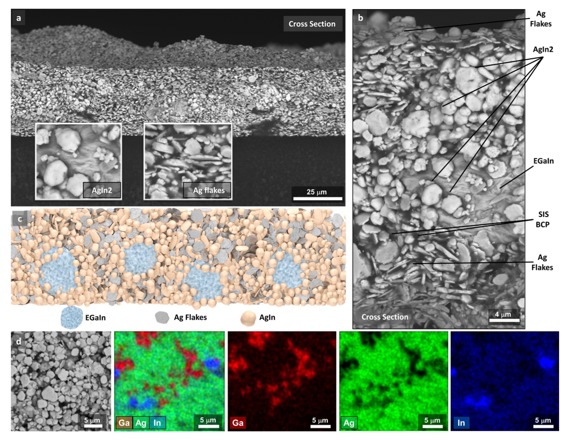
SEM and EDS analysis of ink samples. (a) Cross section of a printed sample. EGaIn droplets, Ag flakes, and newly formed AgIn2 microparticles are visible (SEM BSE) (25 μm scale bar). (b) Cross-sectional image at higher magnification, showing EGaIn, Ag microflakes, and AgIn2 (SEM BSE) (4 μm scale bar). (c) Schematic model of the trinary microstructure. AgIn2 particles are mostly present around liquid GaIn, while the remaining Ag flakes that did not form AgIn2 are distributed in the sample. (d) (SEM BSE and EDS) Elemental analysis of the sample and distribution of Ga, In, and Ag in the microstructure (5 μm scale bars).
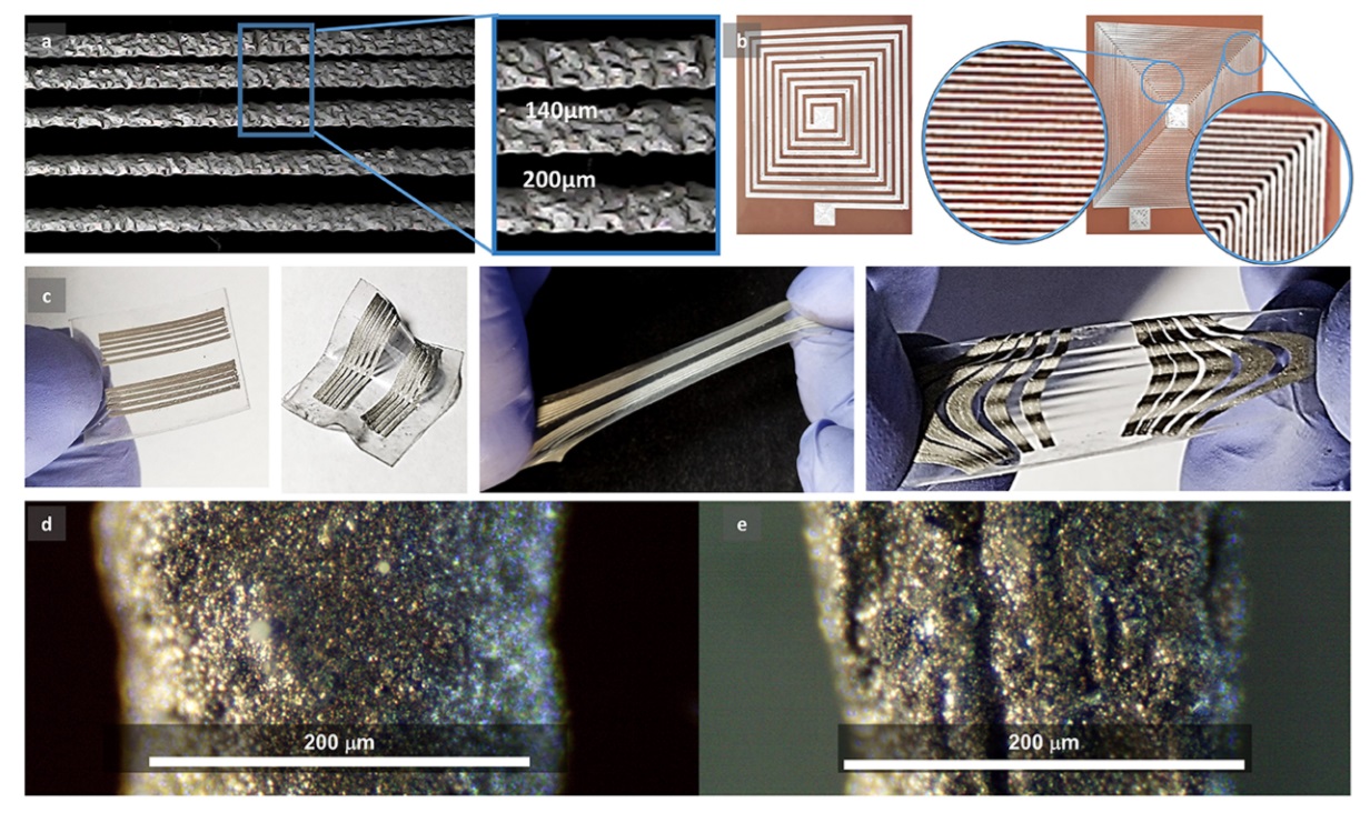
Printing resolution. (a) Photo of 200 μm lines printed over an SIS substrate with varying spacing. (b) Coils printed over a Kapton substrate with 1 mm (left) and 200 μm line widths. (c) Example of printed lines over the SIS layer and the same sample under stretch (right). (d) Optical microscopy image of a printed line in rest and (e) during ∼50% strain (200 μm scale bars).


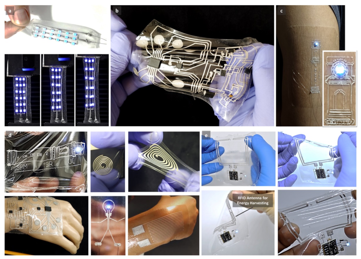
Examples of digitally printed stretchable circuits. (a) Matrix of LEDs under strain. (b) Multi-layer stretchable circuit made over an SIS substrate. Here, the SIS prepolymer is applied with a desired thickness, using a thin-film applicator, prior to the printing of each layer. (c) Circuit printed over the Tegaderm medical adhesive and transferred to the skin with LED powered on. (d) Examples of various printed circuits, including a strain gauge for the monitoring of the wrist bending and a circular coil. (e) Fully wireless circuit, composed of an RFID antenna for energy harvesting, a radio frequency to direct current module, and an LED, operated at 1 m distance from the transmitter, without battery.
The AgInGa-SIS ink and extrusion-based printing method represents an important step toward a universal approach for the rapid and scalable fabrication of stretchable electronics with complex multi-layer circuit architectures. Due to the simplicity, low cost, and widespread use of extrusion-based printers, extrusion printing of a resilient and stretchable ink is an enabling technology for further progress and customization in other fields of research and application. In particular, the AgInGa-SIS ink could be utilized for 3D-printed hybrid devices with embedded circuitry, customized e-textile, organ-interfacing bioelectronics, pressure-mapping films, soft robots, and printed sensors and antennas. It can also enable the facile fabrication of customized current collector designs for use in thin-film batteries and energy harvesting systems that are soft, flexible, and stretchable.
Bi-Phasic Ag–In–Ga-Embedded Elastomer Inks for Digitally Printed, Ultra-Stretchable, Multi-layer Electronics
DOI: 10.1021/acsami.0c22206

