

Reversible polymer-gel transition for ultrastretchable chip-integrated circuits through self-soldering and self-coating and self-healing
Pedro Alhais Lopes
Bruno C. Santos
Aníbal T. de Almeida
Mahmoud Tavakoli
Integration of solid-state microchips into soft-matter, and stretchable printed electronics has been the biggest challenge against their scalable fabrication. We introduce, Pol-Gel, a simple technique for self-soldering, self-encapsulation, and self-healing, that allows low cost, scalable, and rapid fabrication of hybrid microchip-integrated ultra-stretchable circuits. After digitally printing the circuit, and placing the microchips, we trigger a Polymer-Gel transition in physically cross-linked block copolymers substrate, and silver liquid metal composite ink, by exposing the circuits to the solvent vapor. Once in the gel state, microchips penetrate to the ink and the substrate (Self-Soldering), and the ink penetrates to the substrate (Self-encapsulation). Maximum strain tolerance of ~1200% for printed stretchable traces, and >500% for chip-integrated soft circuits is achieved, which is 5x higher than the previous works. We demonstrate condensed soft-matter patches and e-textiles with integrated sensors, processors, and wireless communication, and repairing of a fully cut circuits through Pol-Gel.
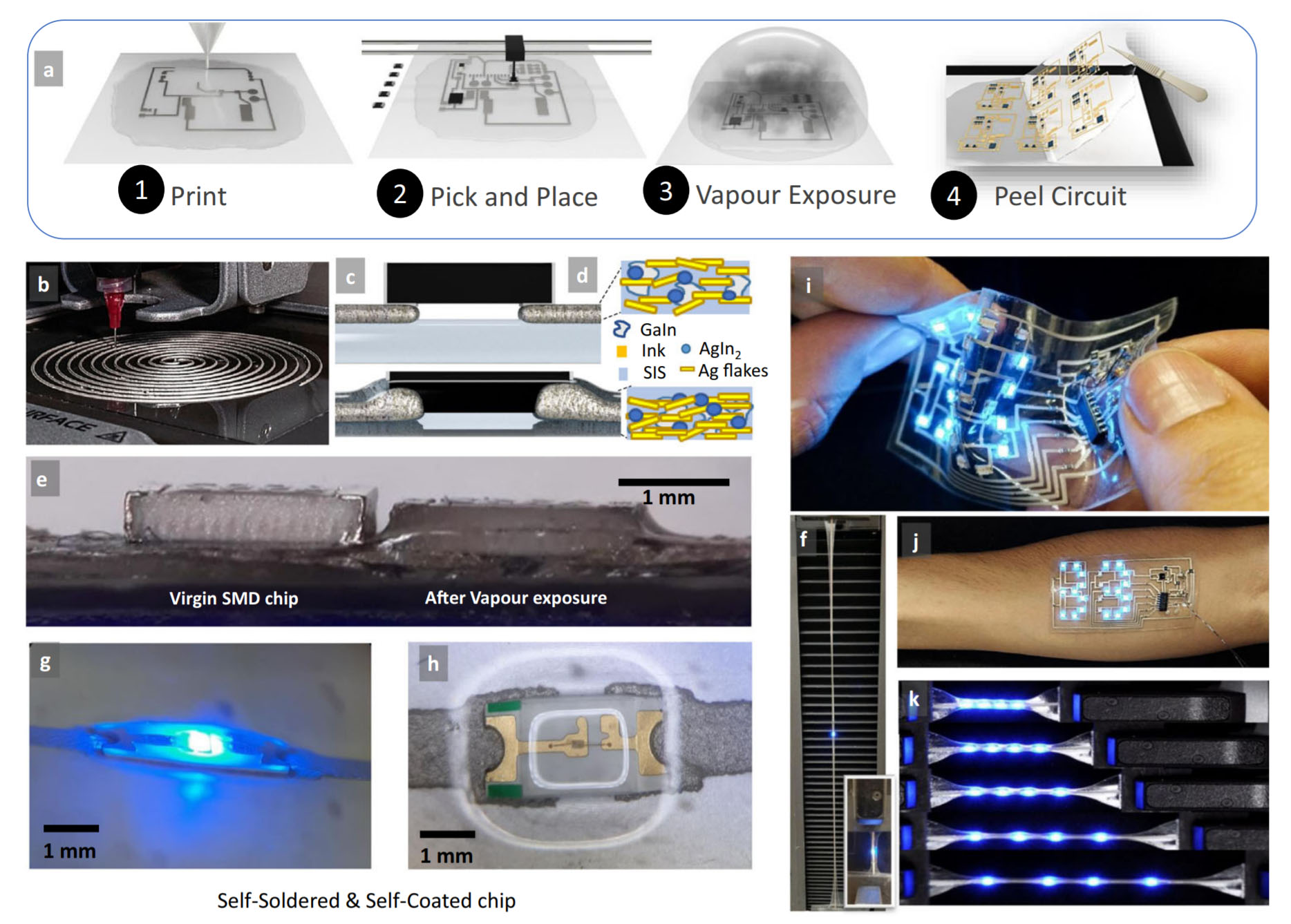
Fabrication process for hybrid stretchable circuits.
a) Process for chip-integrated circuit fabrication. Printing using an extrusion printer and the
Ag–In–Ga–SIS ink, pick and place of microchips, Pol–Gel transition through solvent vapor exposure, and peeling of the circuit.
b) Example of a digitally
printed circuit with 14 layers of ink.
c) Schematics of the chip interfacing through Pol–Gel.
d) Schematics of the ink microstructure before and after vapor
exposure.
e) Side view of a small resistor chip before and after vapor exposure.
f) A sample with an integrated LED, after being cut, and healed through
Pol–Gel, <900% strain.
g) Side view of a self-encapsulated circuit through Pol–Gel.
h) Top view of a self-encapsulated circuit through Pol–Gel.
i) Soft-matter
circuit with integrated sensors, microprocessor, and LED display for temperature measurement.
j) Same circuit was applied to the skin. k Example of a
circuit with multiple LEDs
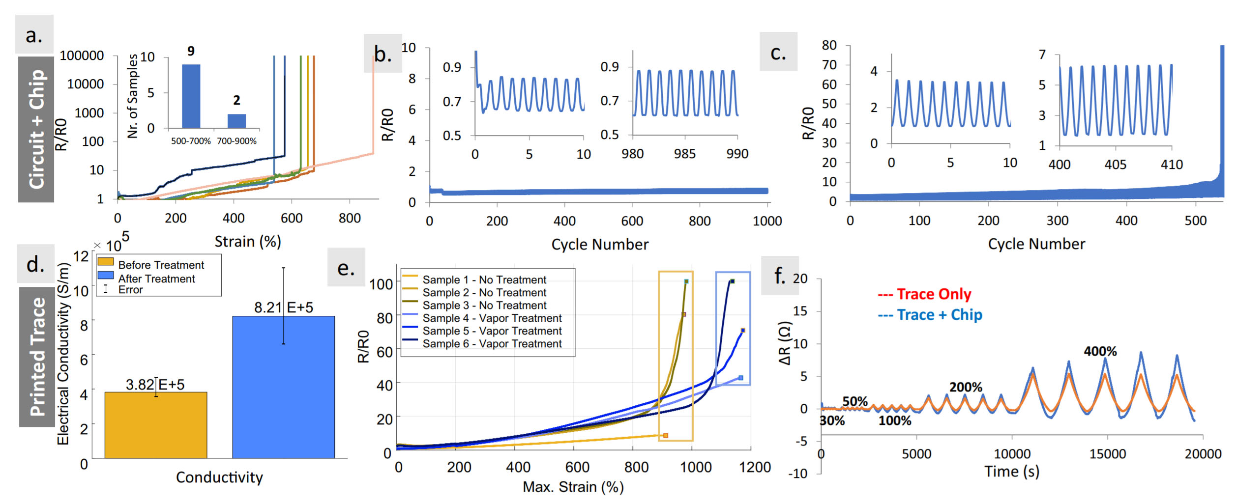
Electromechanical characterization.
a) Max. strain tolerance of multiple samples with an integrated resistor package.
b) One hundred percent strain
cycle of the chip-integrated sample.
c) Four hundred percent strain cycle of the chip-integrated sample.
d) Conductivity of printed traces before and after the
Pol–Gel.
e) Maximum strain tolerance of the printed traces before and after the Pol–Gel.
f) Electrical resistance comparison of a printed trace without and
with integrated chip, under strains of 30, 50, 100, 200, and 400%.
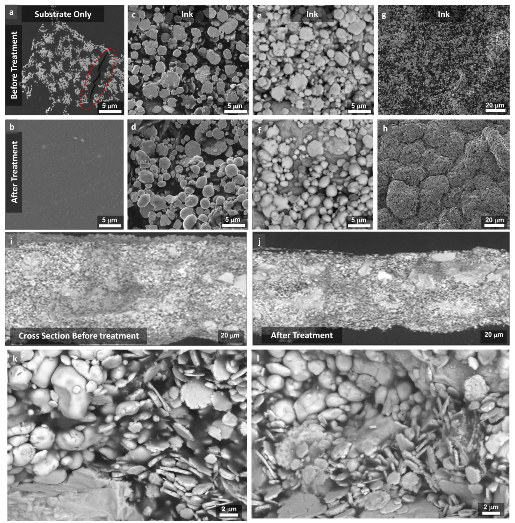
Scanning electron microscopy.
SEM of the substrate and the printed ink before and after vapor exposure.
SIS substrate before (a) and after (b) the
exposure. The SE images of the ink before (c) and after exposure (d). The BSE images of the ink before (e) and after exposure (f). Highly diluted ink spray
coated over the textile before (g) and after (h) vapor exposure. Cross section of SEM images of the printed ink before (i, k) and after vapor exposure (j, l).
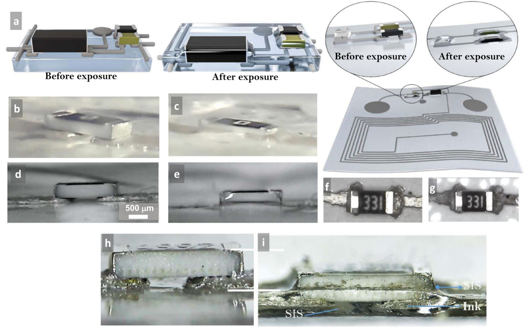
Details of the self-soldering process.
(a) A schematic presentation of the microchip integration into the soft-matter circuit before and after exposure. Snapshot of a resistor component before (b) and after vapor exposure (c). Note the penetration of the component and the ink into the substrate. Side view of a resistor chip before (d) and after (e) vapor exposure. The light reflection of the chip after exposure shows the SIS that climbed the walls of the chip due to capillary action. Top view of the resistor chip before (f) and after (g) vapor exposure. The color difference of the ink demonstrates encapsulation. Magnified side view of the resistor chip before (h) and after (i) vapor exposure. All of the ink and approximately half of the resistors are inside the substrate. Note also the SIS below the resistor and on the sides.
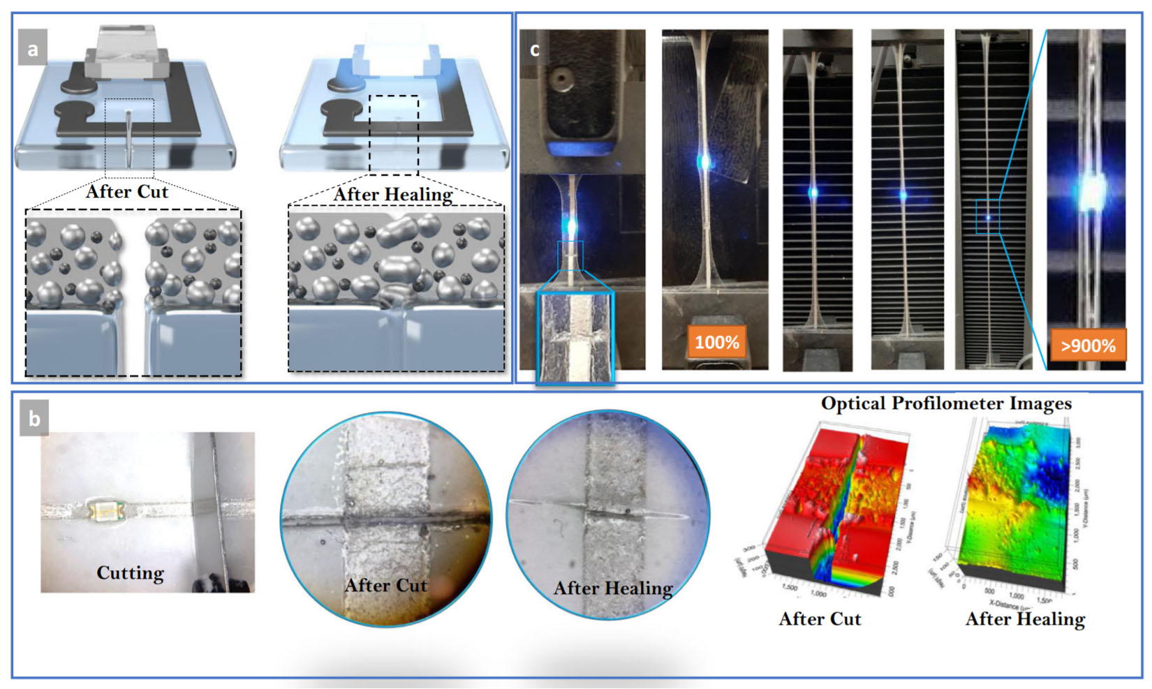
The self-healing process.
a) Schematics of the healing process.
b) Image from the sample undercut, after a deep cut of the ink and the substrate, and after healing through vapor exposure. Optical profilometer images of the cut before and after healing.
c) A dully cut and healed sample under tensile strain test of 900%, and the magnified image of the sample prior to breaking.
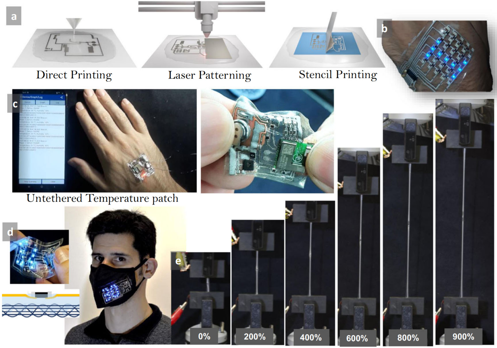
Circuit patterning techniques and examples of applications.
a) Soft-matter circuit with Ag–In–Ga–SIS ink can be produced by extrusion printing, fiber laser patterning, or stencil printing.
b) Example of an LED display with 60 integrated chips fabricated by extrusion printing and vapor exposure.
c) Anuntethered wireless temperature patch with integrated Bluetooth chip, temperature and humidity sensor, microprocessor, resistors, and battery, produced through laser patterning and vapor exposure. The patch sends the data to the mobile phone app.
d) A condensed soft-matter circuit with temperature sensor and LED display matrix, transferred to the textile through the same Pol–Gel procedure. During the gel state, the SIS substrate penetrates into the fibers of the e-textile, resulting in seamless integration. e Example of a sample with a resistor chip <0–900% strain. The authors affirm that the human research participant (first author P.L.) provided informed consent for publication of the images in (b–d).
Reversible polymer-gel transition for ultrastretchable chip-integrated circuits through self-soldering and self-coating and self-healing
Lopes, P.A., Santos, B.C., de Almeida, A.T. et all. Reversible polymer-gel transition for ultra-stretchable chip-integrated circuits through self-soldering and self-coating and self-healing. Nat commun 12, 4666 (2021). https://doi.org/10.1038/s41467-021-25008-5