

3R Electronics: Scalable Fabrication of Resilient, Repairable, and Recyclable Soft-Matter Electronics
Mahmoud Tavakoli
Pedro Alhais Lopes
Abdollah Hajalilou
André F. Silva
Manuel Reis Carneiro
José Carvalheiro
João Marques Pereira
Aníbal T. de Almeida
E-waste is rapidly turning into another man-made disaster. It is proposed that a paradigm shift toward a more sustainable future can be made through soft-matter electronics that are resilient, repairable if damaged, and recyclable (3R), provided that they achieve the same level of maturity as industrial electronics. This includes high-resolution patterning, multilayer implementation, microchip integration, and automated fabrication. Herein, a novel architecture of materials and methods for microchip-integrated condensed
soft-matter 3R electronics is demonstrated. The 3R function is enabled by a biphasic liquid metal-based composite, a block copolymer with nonpermanent physical crosslinks, and an electrochemical technique for material recycling. In addition, an autonomous laser-patterning method for scalable circuit patterning with an exceptional resolution of <30 µm in seconds is developed. The phase-shifting property of the BCPs is utilized for vaporassisted “soldering” circuit repairing and recycling. The process is performed
entirely at room temperature, thereby opening the door for a wide range of heat-sensitive and biodegradable polymers for the next generation of green electronics. The implementation and recycling of sophisticated skin-mounted patches with embedded sensors, electrodes, antennas, and microchips that build a digital fingerprint of the human electrophysiological signals is demonstrated by collecting mechanical, electrical, optical, and thermal data from the epidermis.
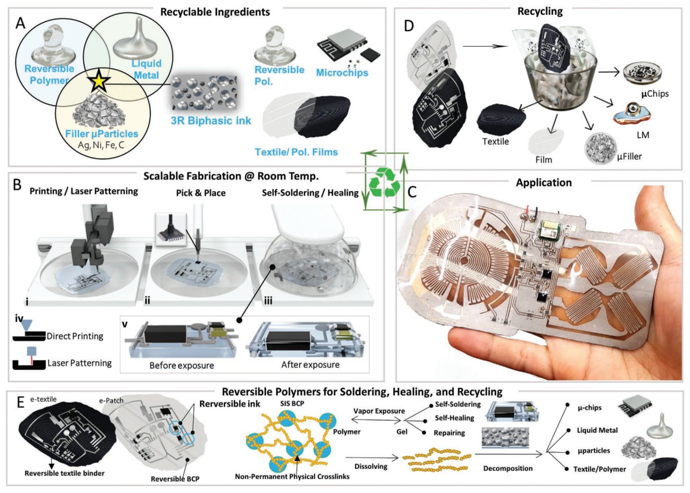
3R Electronics. A) Constitutional materials, including biphasic liquid metal-based inks and reversible polymers. B) Autonomous fabrication techniques including printing/laser patterning i), Pick and place ii), and vapor-assisted soldering and healing iii). Thanks to the reversible polymers, the microchips penetrate the ink and the substrate, resulting in a seamless integration into the circuit v). C) Example of a laser patterned soft-matter circuit with eight strain gauges and state of the art SMD microchips for processing, amplification, and communication. D) The concept for recovery of the elements from 3Rs electronics, based on dissolving reversible polymeric matrix. E) Utilization of reversible polymers with nonpermanent physical crosslinks, as the substrate, e-textile adhesive, and binder in ink, contributes to self-soldering, Self-healing, repairing and recycling.
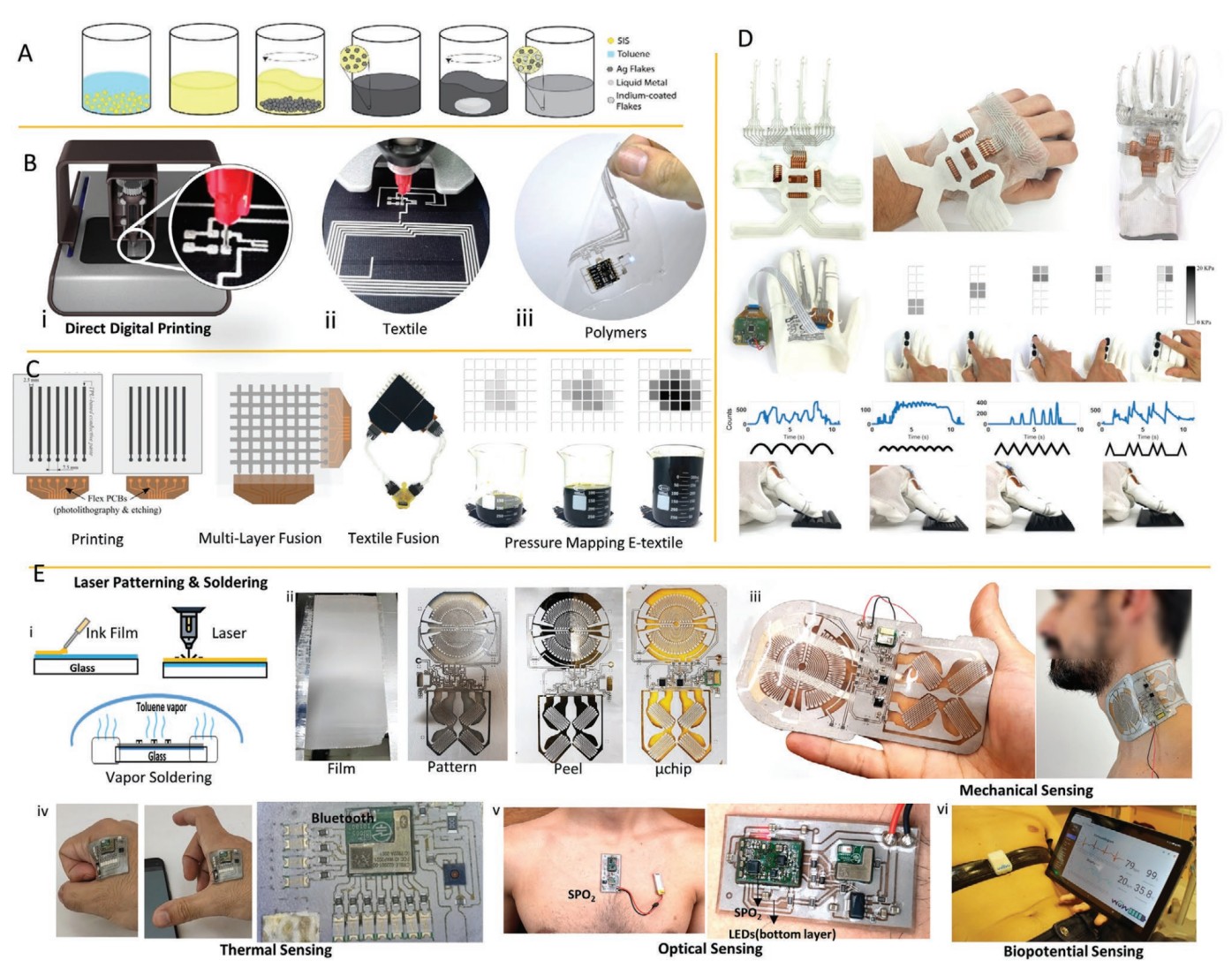
A) Synthesis of sinter-free stretchable biphasic ink. B) Digital Printing of e-patch and e-textile circuits C) Example of a pressure mapping e-textile fabricated through digital printing. D) Example of a wearable glove with printed bending and pressure sensors, its application in pressure sensing, and surface texture classification. E) High-resolution Laser Patterning of the circuits using an accessible IR laser and Single-step vapor-assisted soldering of miniaturized components: i) Example of the fabrication steps. ii) No solder material or thermal treatment is necessary. Examples of chipintegrated soft-matter epidermal biostickers for mechano-sensing iii), thermal iv), optical v), and electrical sensing vi). These patches can be used for monitoring respiration and physical activities iii), body temperature iv), heart rate, and SPO2 v). The belt presented in E-iv measures ECG, heart rate, respiration, temperature, and body motions simultaneously.
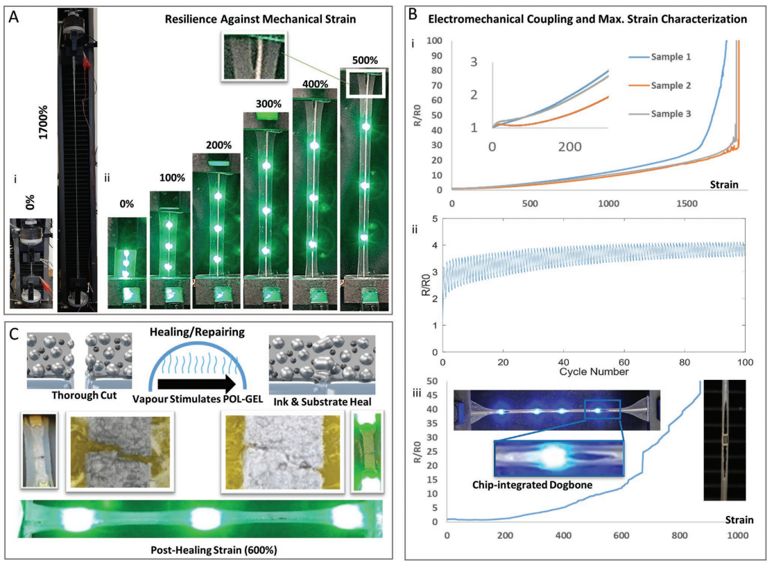
A) Printed trace without chip i) and with microchips ii) under strain. B) Electromechanical coupling of the circuits. Electrical resistance versus strain (i), repetitive cycle test for 30% strain ii), resistance v/s strain for microchip integrated circuit iii). Cracks are formed usually at >500% strain on the substrate and grow until mechanical failure. C) Vapor-assisted repairing of the circuit which was cut using a sharp knife, and the same circuit under 600% strain after healing.
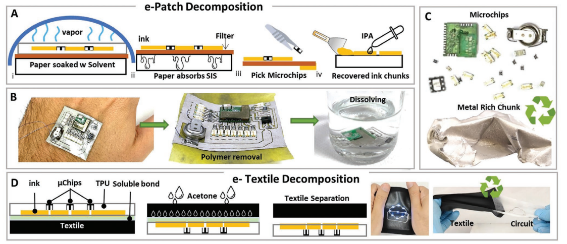
Recycling the e-patch and e-textile circuits. A) e.patch are first decomposed by a vapor-assisted substrate removal, allowing separation of the microchips and ink as a metal chunk. B) Example of wireless thermal monitoring patch on the skin, after polymer removal. An alternative method for removing components and the ink is direct dissolving. C) Microchips, battery, and metal chunk removed from the thermal patch. D) e-textile recycling starts with removing the acetone soluble bond between the e-patch and the textile. After the recovery of the textile, the e-patch is recycled using the same technique as (A).
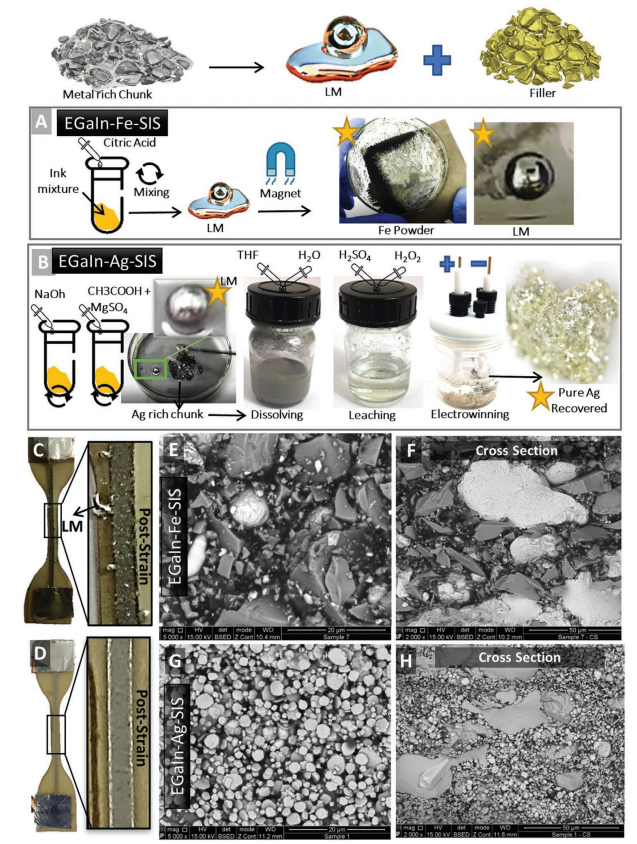
Extraction of the metal elements from the recovered metal chunk in the previous step. A) Method for separation of LM and Ferrite from EGaIn–Fe metal chunk, using magnetic force. B) Method for separation of Ag, and EGaIn, based on the mechano-chemical procedure followed by dissolving, leaching and Electrowinning. C) Fe–EGaIn–SIS composite after 100% mechanical strain. The phase separation is expectable due to the nonhomogeneous microstructure as shown in SEM analysis: E) top surface and F) cross-section. D) Optical image of an Ag–EGaIn–SIS sample poststrain. SEM microscopy from G) top surface and H) Cross-section
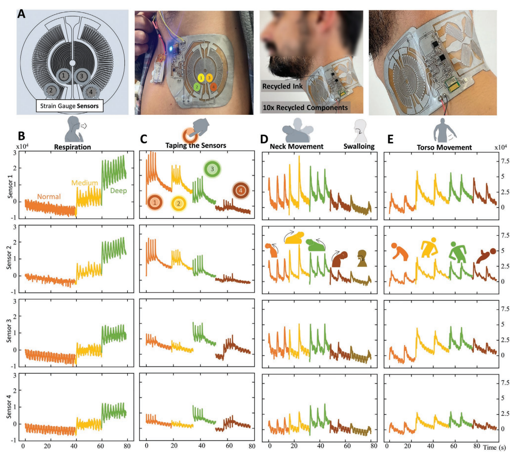
A) Soft-matter chip-integrated multinode sensor patch produced by 1× recycled LM and 10× recycled microchip. Fingerprint of the generated signal during mild, normal, and deep respiration (B), tapping (C), four different neck movements, and swallowing (D), and four different torso movement (E).
3R Electronics: Scalable Fabrication of Resilient, Repairable, and Recyclable Soft-Matter Electronics
https://doi.org/10.1002/adma.202203266