

EGaIn-Assisted Room-Temperature Sintering of Silver Nanoparticles for Stretchable, Inkjet-Printed, Thin-Film Electronics
People involved:
- Mahmoud Tavakoli
- Mohammad H. Malakooti
- Hugo Paisana
- Yunsik Ohm
- Daniel Green Marques
- Pedro Alhais Lopes
- Ana P. Piedade
- Anibal T. de Almeida
- Carmel Majidi
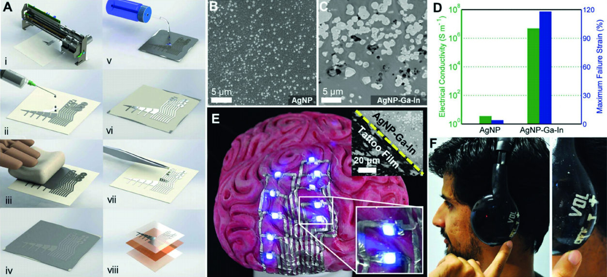
Soft, stretchable, and ultrathin printed electronics for 3D hydrographic printing: A) printing procedure of conductive traces. B) SEM of inkjetprinted silver nanoparticles. C) SEM of “sintered” silver nanoparticles and liquid metal alloy. D) volumetric electrical conductivity and maximum failure strain of AgNP coating prior and after EGaIn deposition. E) Hydrographically transferred electronic tattoo on a model brain; (top inset: micrograph of AgNP-Ga-In circuit trace and exposed tattoo film, bottom inset: Light-emitting diodes (LEDs) having different orientation on the highly textured surface). F) Conformal capacitive touchpad on a headphone created using hydrographic transfer technique.
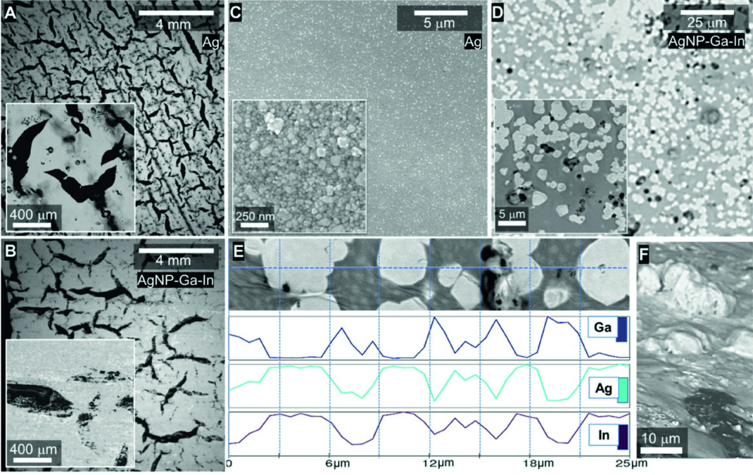
Characterization of printed AgNP and AgNP-Ga-In traces; A) microcracks in printed AgNP, B) reduced crack density after EGaIn deposition, microscopy images of: C) printed AgNP and D) EGaIn-coated AgNP on temporary tattoo film. E) Energy-dispersive X-ray spectroscopy (EDS) line analysis of the conductive traces with bright and Gray coating regions. F) Formation of Ag-Ga-In “mountains” over Ga rich areas.
Characterization of printed AgNP and AgNP-Ga-In traces; A) microcracks in printed AgNP, B) reduced crack density after EGaIn deposition, microscopy images of: C) printed AgNP and D) EGaIn-coated AgNP on temporary tattoo film. E) Energy-dispersive X-ray spectroscopy (EDS) line analysis of the conductive traces with bright and Gray coating regions. F) Formation of Ag-Ga-In “mountains” over Ga rich areas.
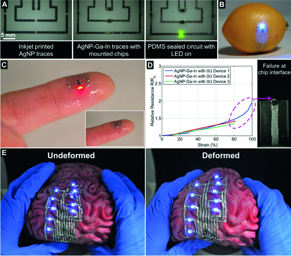
Conductive AgNP-Ga-In traces for flexible electronics: A) Process for populating AgNP-Ga-In circuit with surface mounted components, B) circuit placed on a toy lemon using hydrographic transfer, C) circuit functioning as electronic tattoo on human skin with an integrated LED on finger print, inset: LED is off on the same circuit, D) relative resistance versus strain of conductive traces with a 0 Ω resistor in the middle of specimen, subjected to uniaxial strain until mechanical failure, inset: failed specimen at the interface between chip and PDMS. E) Functioning LEDs on a soft brain-shaped toy before and after deformation (see Video S3, Supporting Information).
EGaIn‐Assisted Room‐Temperature Sintering of Silver Nanoparticles for Stretchable, Inkjet‐Printed, Thin‐Film Electronics
M. Tavakoli et all.. “EGaIn-Assisted Room-Temperature Sintering of Silver Nanoparticles for Stretchable, Inkjet-Printed, Thin-Film Electronics”, 2018, 30, 1801852