

Hydroprinted Electronics:
People involved:
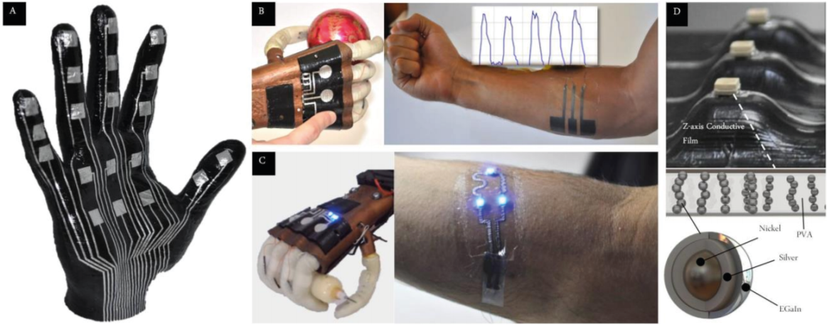
Hydroprinted Electronics. A). Example of capacitive proximity sensor mesh printed over the transfer paper and hydroprinted over a 3D printed hand model B). Example of a functional printed circuit, hydroprinted over 3D printed shell of a prosthetic hand and electronic tattoos over the human skin for acquiring bio potentials C) The ultrathin carrier film of the TTP can be populated with SMD chips prior to transfer thanks to the anisotropic zPVA matrix developed in this work. D) The zPVA interface is composed of Ag-coated Ni particles with additional EGaIn oating layer, in a PVA gel. These particles form conductive columns that conduct electricity only on the Z- axis, which facilitates interfacing of small SMD components.
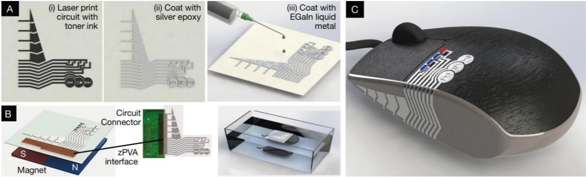
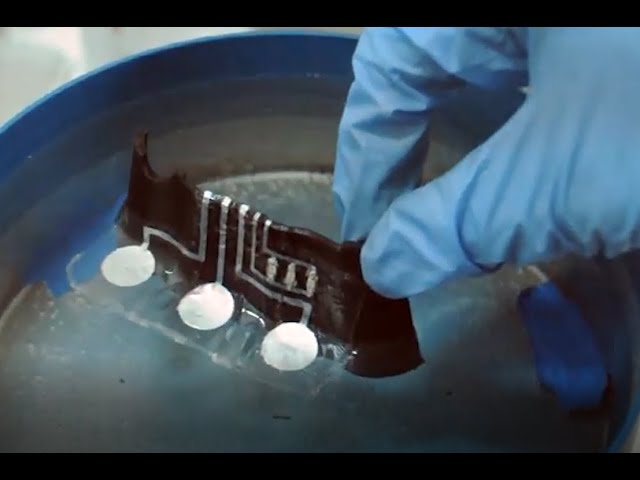
Fabrication Steps Overview. Fabrication can include printing, interfacing with microelectronic chips or external circuits, and Hydroprinting. After printing the pattern with a desktop laser printer (A-i), the circuit template is coated with subsequent layers of Ag paste (Aii), and EGaIn alloy (A-iii). The excess metallic coatings are rinsed away after each deposition step. Surface-mounted electronics, or external circuits are connected using an anisotropic “zPVA glue” (B). Finally, the circuit can be transferred over a surface using hydrographic transfer (C).
Hydrographics Transfer method and applications for a prosthetic hand. A). Process for Hydroprinting of the thin film electronics composed of capacitive tactile input sensors and surface mount LEDs over the 3D printed shell of the prosthetic hand, including B). Process for application of an electronic tattoo over the forearm for EMG signal acquisition C). The hand can be controlled by EMG input or by hydroprinted circuit over the hands shell. That contains tactile inputs and surface mount LEDs for reciprocal human machine interaction.
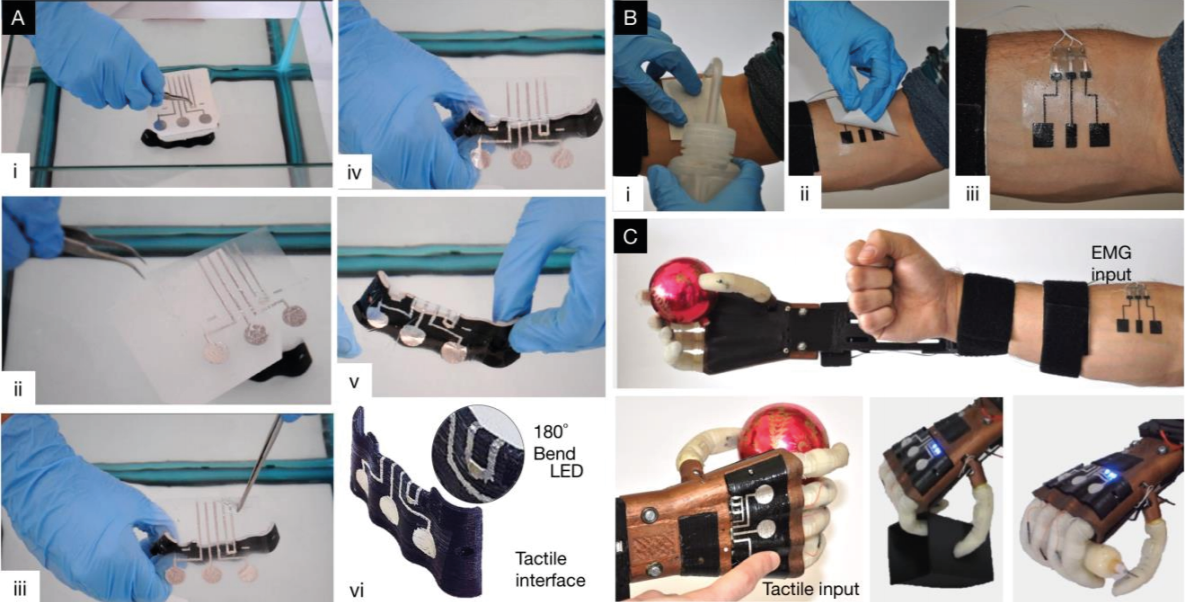
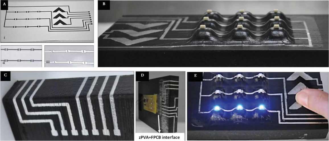
Printed “Ag-In-Ga” circuit with capacitive proximity sensors and LEDs transferred over a complex 3D surface. A). Initial print with a laser printer (i), after silver epoxy deposition (ii), and after EGaIn deposition (iii). B). Circuit transferred over the 3D printed part C). During the transfer, interconnects bend over and effectively adhere to the host surface D). The end points are then interfaced with a PCB through a flex circuit and zPVA E). Final circuit: Hand proximity turns the LEDs on.