

Reliable interfaces for EGaIn multi-layer stretchable circuits and microelectronics.
People involved:
Daniel Green Marques
Pedro Alhais Lopes
Anibal T de Almeida
Carmel Majidi
Mahmoud Tavakoli
We tackle two well-known problems in the fabrication of stretchable electronics: interfacing soft circuit wiring with silicon chips and fabrication of multi-layer circuits. We demonstrate techniques that allow integration of embedded flexible printed circuit boards (FPCBs) populated with microelectronics into soft circuits composed of liquid metal (LM) interconnects. These methods utilize vertical interconnect accesses (VIAs) that are produced by filling LM alloy into cavities formed by laser ablation. The introduced technique is versatile, easy to perform, clean-room free, and results in reliable multi-layer stretchable hybrid circuits that can withstand over 80% of strain. We characterize the fabrication parameters of such VIAs and demonstrated several applications, including a stretchable touchpad and pressure detection film, and an allintegrated multi-layer electromyography (EMG) circuit patch with five active layers including acquisition electrodes, on-board processing and Bluetooth communication modules.
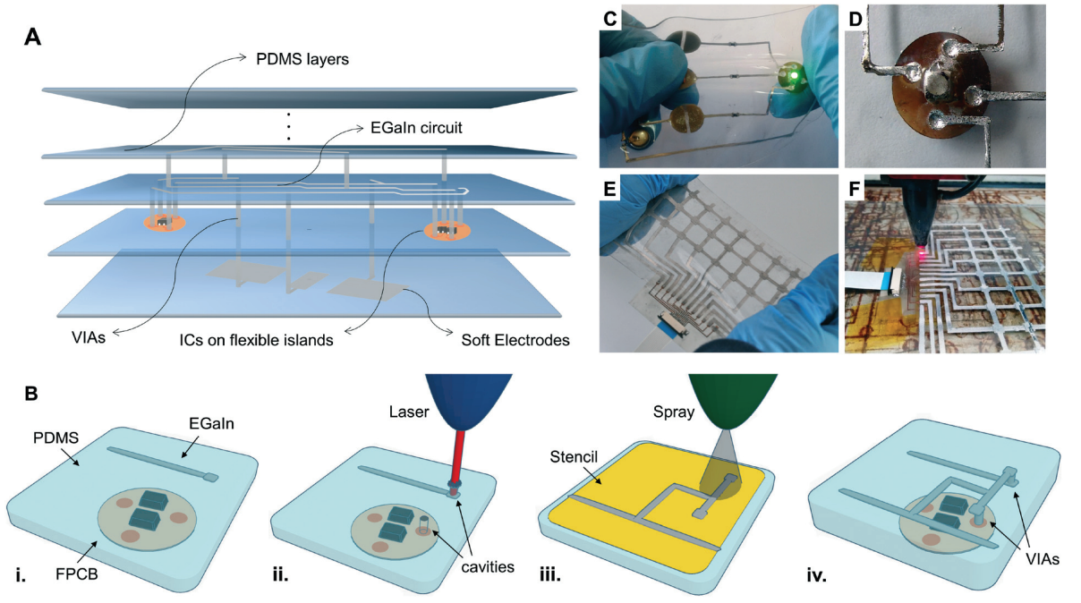
A. Exploded view drawing of a multi-layer stretchable circuit with interfaced microelectronics and flexible islands with a bottom layer for soft electrodes. Additional layers and VIAs can be fabricated; B. fabrication of EGaIn VIAs: (i.) once the flexible PCBs and EGaIn interconnects are encapsulated in a stretchable elastomer (ii.) the selected traces and pads are accessed by vertical laser ablation (iii.) the cavities are filled with liquid metal when spray coating over a patterned stencil (iv.), which is removed before encapsulating the VIAs and the new circuit layer; C. stretchable circuit with multi-layer VIAs-based interfaces with a RGB LED soldered on a flexible island with copper pads (FPCB); D. detail view of the LED on a FPCB after simultaneous masked spray deposition of the EGaIn circuit and VIAs; E. soft capacitive touchpad and pressure mapping film interfaced with an external processing unit; F. fabrication step of CO2 laser ablation prior to the deposition of EGaIn VIAs.
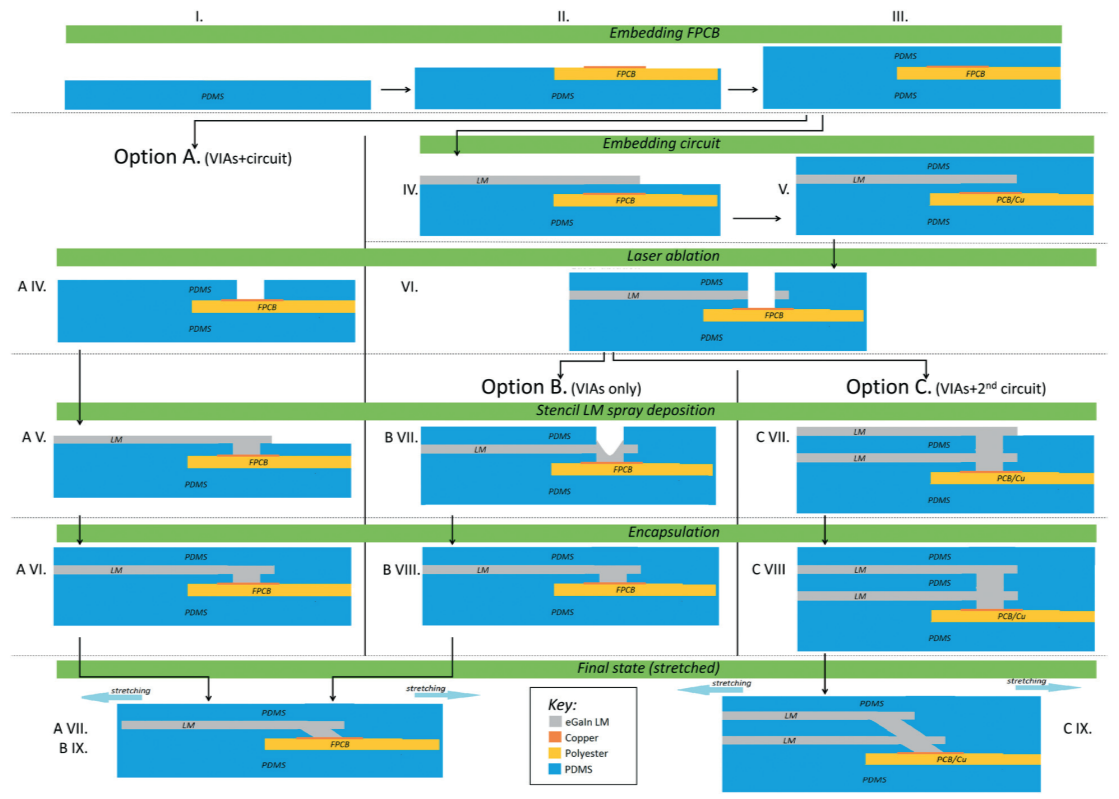
Detailed flow of the processing steps for the creation of a multi-layer interfaces, showing possible variations: (A) simultaneous fabrication of VIAs and the circuit layer; (B) fabrication of VIAs with a previous embedded circuit layer; and (C) fabrication of VIAs and additional circuit layers besides the previous embedded circuit layer. In layer-by-layer manufacture, the FPCB is placed onto a half-cured PDMS substrate (I. and II.) and sealed (III.). Eventually a EGaIn circuit layer is embedded too (IV. and V.). Vertical laser ablation of the elastomer is used to access the bottom Cu layer on the FPCB and any intermediate EGaIn layers (VI. and A IV.). Spray masked deposition of EGaIn fills the VIAs and can create additional circuit layers (A V., B VIII. and C VIII.). Finally a top sealing layer of PDMS is applied to encapsulate the device (A VI., B VIII. and C VIII.). The interfaced system withstands applied stress and deformation (A VII., B IX. and C IX.).
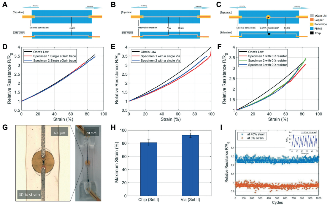
Electromechanical characterization of dedicated samples under tensile loading. Top-view and cross-section schematic views of the specimens: A. EGaIn reference sample (set I); B. single VIA connecting two EGaIn traces (set II); C. SMD 0 Ω chip resistor interfaced with VIAs to EGaIn traces (set III). Relative resistance and strain curve: D. set I; E. set II; F. set III; G. Specimen from set III and detail view of the delamination of a flexible island at 40% uniaxial strain. H. Stretchability of VIAs and interfaces. I. Under cyclic mechanical loading, the interfaced chips (set I) reliably maintain the range of variation over 1000 cycles at 40% and 0.4 Hz. Inset: To a stretch/release cycle corresponds an increase/decrease in resistance due to the EGaIn interconnects.
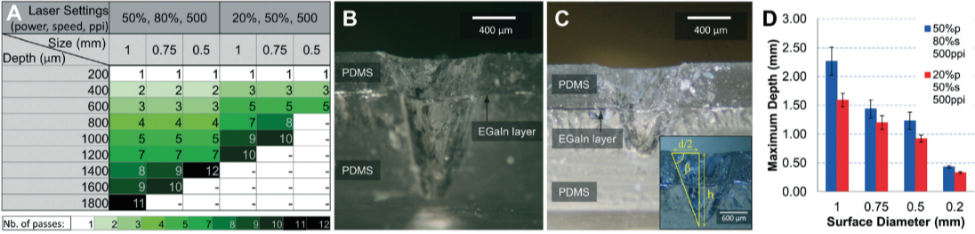
A. Number of passes to reach a range of depths from 200 to 1800 μm for different ablation surface diameters (size) and laser ablation settings. Microscope view of the cross section of the ablation result for the same number of passes for laser settings 1 and 2 and different surface sizes, presenting its typical cone-shape: B. 50% power, 80% speed, 500 ppi, 1.0 mm top diameter. On successive passes the laser ablates areas out of the beam focus. C. 20% power, 50% speed, 500 ppi, 0.75 mm top diameter. D. Estimated maximum depth for four different surface diam
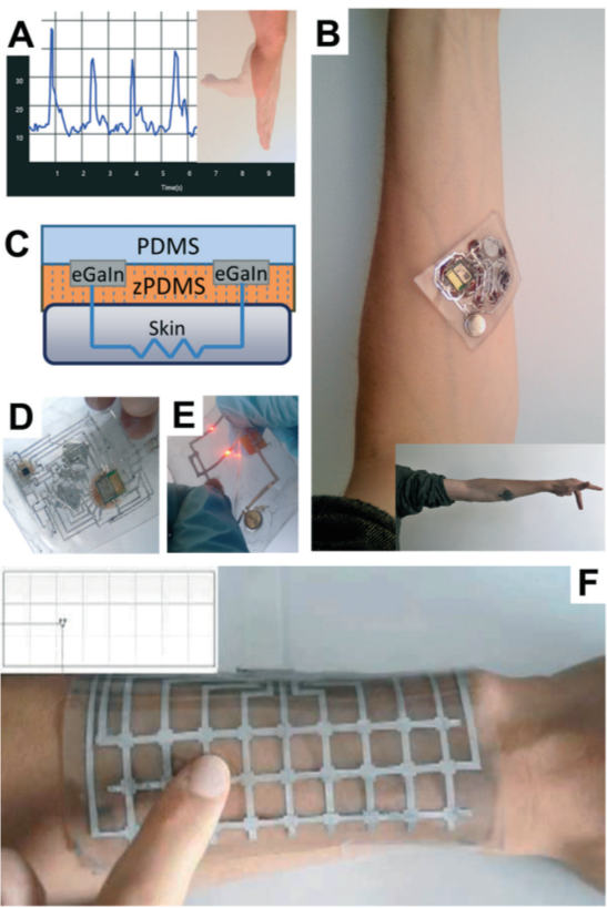
A. EMG signal from a repetitive hand gesture transmitted to a computer application (ESI,† Video); B. all-integrated EMG patch on the forearm. Inset: Adhesion of the EMG patch to the skin while performing a hand gesture; C. cross-view of a z-axis conductive PDMS47 and schematic of the electrical path connecting the separate EGaIn traces and a conductive surface for soft electrodes or buttons; D. EMG patch seen from the bottom; E. double-layer LED circuit with a coin cell battery and a zPDMS button, each LED is on a different circuit layer; F. human– machine interaction with a soft touchpad placed on a volunteer’s forearm to control a display which shows the point of pressure of the finger. The device uses VIAs to interface with the computer.
Reliable interfaces for EGaIn multi-layer stretchable circuits and microelectronics.
M. Tavakoli et all.. “Reliable interfaces for EGaIn multi-layer stretchable circuits and microelectronics“, 10.1039/C8LC01093E, Lab Chip, 2019,19, 897-906